- 您现在的位置:买卖IC网 > Sheet目录2040 > PI74ALVCH16501A (Pericom)IC UNIV BUS TXRX 16BIT 56TSSOP
PI74ALVCH16501
18-BIT UNIVERSAL BUS TRANSCEIVER
2
PS8133A
01/31/00
12345678901234567890123456789012123456789012345678901234567890121234567890123456789012345678901212345678901234567890123456789012123456789012
Pin Name
Description
OE
Output Enable Input (Active HIGH)
LE
Latch Enable (Active HIGH)
CLK
Clock Input (Active HIGH)
Ax
Data I/O
Bx
Data I/O
GND
Ground
VCC
Power
1
2
3
4
5
6
7
8
9
10
11
12
13
14
15
16
17
18
19
20
21
22
23
24
56
55
54
53
52
51
50
49
48
47
46
45
44
43
42
41
40
39
38
37
36
35
34
33
25
26
27
28
32
31
30
29
Product Pin Description
Truth Table(1)
Notes:
1. H = High Signal Level
L = Low Signal Level
Z = High Impedance
↑=LOW-to-HIGHTransition
A-to-B data flow is shown: B-to-A flow is similar but
uses OEBA, LEBA, CLKBA.
Output level before the indicated steady-state input
conditions were established, provided that CLKAB is HIGH
before LEAB goes LOW.
§ Output level before the indicated steady-state input
conditions were established.
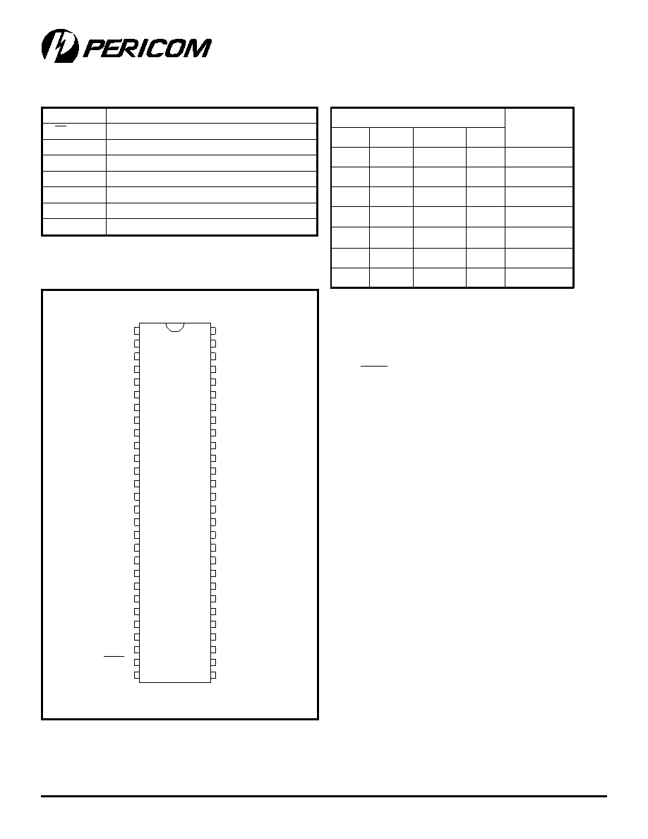
Product Pin Configuration
56-PIN
V-56
A-56
OEAB
LEAB
A1
GND
A2
A3
VCC
A4
A5
A6
GND
A7
A8
A9
A10
A11
A12
GND
A13
A14
A15
VCC
A16
A17
GND
A18
OEBA
LEBA
GND
CLKAB
B1
GND
B2
B3
VCC
B4
B5
B6
GND
B7
B8
B9
B10
B11
B12
GND
B13
B14
B15
VCC
B16
B17
GND
B18
CLKBA
GND
s
t
u
p
n
I
B
t
u
p
t
u
O
B
A
E
OB
A
E
LB
A
K
L
CA
LX
X
Z
HH
X
L
HH
X
H
HL
↑
LL
HL
↑
HH
HL
H
X
B0
HL
L
X
§
0
B
发布紧急采购,3分钟左右您将得到回复。
相关PDF资料
PI74ALVCH16646A
IC TRANSCVR DUAL N-INV 56TSSOP
PI74ALVCH16652A
IC 16-BIT BUS TXCVR/REG 56-TSSOP
PI74ALVCH16721A
IC 20-BIT FLIP-FLOP 56-TSSOP
PI74ALVCH16823A
IC 18-BIT INTERFACE-F/F 56-TSSOP
PI74ALVCHR162245AEX
IC TXRX 16BIT BIDIR 3ST 48TSSOP
PI74ALVTC16241A
IC BUFF DVR TRI-ST 16BIT 48TSSOP
PI74ALVTC16244K
IC BUFF DVR TRI-ST 16BIT 48TVSOP
PI74ALVTC16245A
IC 16-BIT BIDIR TXCVR 48-TSSOP
相关代理商/技术参数
PI74ALVCH16501V
制造商:未知厂家 制造商全称:未知厂家 功能描述:18-Bit Bus Transceiver
PI74ALVCH16524
制造商:未知厂家 制造商全称:未知厂家 功能描述:Logic | 18-Bit Registered Bus Exchanger
PI74ALVCH16524A
制造商:未知厂家 制造商全称:未知厂家 功能描述:18-Bit Bus Transceiver
PI74ALVCH16524V
制造商:未知厂家 制造商全称:未知厂家 功能描述:18-Bit Bus Transceiver
PI74ALVCH16543
制造商:未知厂家 制造商全称:未知厂家 功能描述:Logic | 16-Bit Registered Transceiver
PI74ALVCH16543A
制造商:未知厂家 制造商全称:未知厂家 功能描述:Dual 8-bit Bus Transceiver
PI74ALVCH16543V
制造商:未知厂家 制造商全称:未知厂家 功能描述:Dual 8-bit Bus Transceiver
PI74ALVCH16600
制造商:未知厂家 制造商全称:未知厂家 功能描述:Logic | 18-Bit Universal Bus Transceiver